


Semiconductor manufacturing is a highly sophisticated and precision - driven industry that has witnessed remarkable technological advancements over the years. Among the numerous technologies and equipment that contribute to this field, the Excimer System plays a pivotal and multi - faceted role. As a supplier of Excimer Systems, I have witnessed firsthand how these systems have become indispensable in semiconductor manufacturing processes.
1. Understanding the Excimer System
An Excimer System is a specialized piece of equipment that generates excimer lasers or utilizes excimer lamps. Excimers are short - lived molecules formed from noble gas atoms and halogen atoms. When excited, these molecules can emit intense ultraviolet (UV) light at specific wavelengths. The Excimer System typically consists of a laser or lamp source, optical components for beam shaping and delivery, and control systems to manage the output parameters.
2. Photolithography: The Heart of Semiconductor Fabrication
Photolithography is the cornerstone of semiconductor manufacturing, a process used to transfer circuit patterns onto semiconductor wafers. The Excimer System is a key player in this process. Traditional photolithography techniques using mercury lamps had limitations in terms of resolution and throughput. However, excimer lasers, especially those operating at wavelengths of 248 nm (KrF) and 193 nm (ArF), have revolutionized photolithography.
The short wavelengths of excimer lasers allow for much higher resolution, enabling the creation of smaller and more complex circuit patterns on semiconductor wafers. With the ever - increasing demand for smaller and more powerful semiconductor devices, such as those in smartphones, laptops, and high - performance computing systems, the ability to fabricate nanoscale features is crucial. The Excimer Equipment used in photolithography can precisely control the laser beam's energy, pulse duration, and repetition rate, ensuring consistent and accurate pattern transfer.
For example, in advanced semiconductor nodes, such as 7 nm and below, extreme ultraviolet (EUV) lithography is starting to be adopted. However, excimer lasers are still used as a pre - cursor in some EUV systems to generate plasma, which then emits EUV light. This shows the continued relevance of excimer technology in the most advanced semiconductor manufacturing processes.
3. Annealing and Surface Modification
Another important application of the Excimer System in semiconductor manufacturing is annealing. Annealing is a heat - treatment process used to relieve stress, improve crystal structure, and activate dopants in semiconductor materials. Excimer lasers can perform rapid thermal annealing (RTA) with high precision.
The short - pulse nature of excimer lasers allows for extremely fast heating and cooling cycles, which minimizes the diffusion of dopants and reduces thermal damage to the surrounding areas. This is particularly important in the fabrication of thin - film transistors (TFTs) used in displays and high - performance integrated circuits. By using an Excimer Lamp or laser, the surface properties of semiconductor materials can also be modified. For instance, the UV light can be used to clean the wafer surface, removing organic contaminants and native oxides. This surface cleaning is essential for ensuring good adhesion between different layers of materials during the semiconductor manufacturing process.
4. Deposition and Etching
Excimer Systems also play a role in deposition and etching processes. In chemical vapor deposition (CVD), excimer lasers can be used to activate chemical reactions at lower temperatures. This is beneficial because it reduces the thermal budget of the semiconductor manufacturing process, which is important for preventing damage to sensitive materials and structures.
In etching, excimer lasers can be used for dry etching processes. The high - energy UV light can break chemical bonds in the semiconductor material, allowing for precise removal of material. This dry etching method offers better control over the etching rate and profile compared to traditional wet etching methods, especially for high - aspect - ratio features.
5. Quality Control and Inspection
Quality control is of utmost importance in semiconductor manufacturing. Excimer Systems can be used in inspection processes. The UV light from excimer lamps or lasers can be used to detect defects on the semiconductor wafer surface. The light is scattered or absorbed differently by defective areas compared to normal areas, allowing for the identification of particles, scratches, and other imperfections.
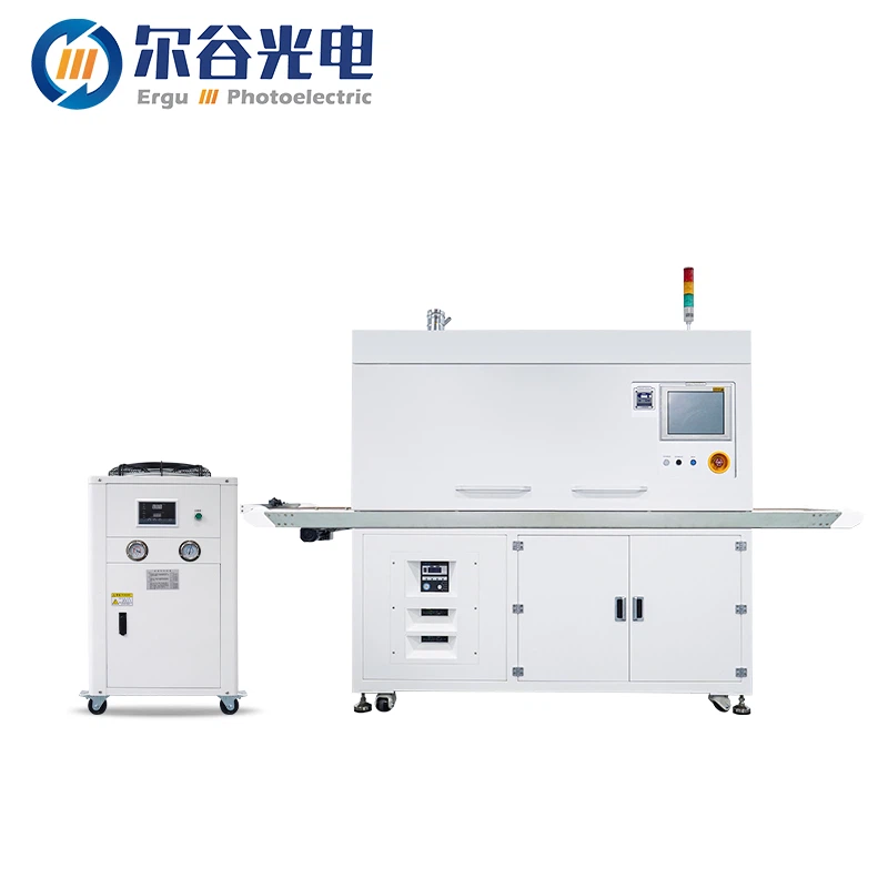

By using advanced imaging techniques in combination with excimer - based illumination, high - resolution inspection systems can be developed. These systems can quickly and accurately detect even the smallest defects, ensuring that only high - quality semiconductor devices are produced.
6. Advantages of Our Excimer Systems
As a supplier of Excimer Systems, we offer several advantages. Our systems are designed with the latest technology to ensure high performance and reliability. We have a team of experienced engineers who can customize the Excimer System according to the specific requirements of semiconductor manufacturers.
Our Excimer Systems are energy - efficient, which helps to reduce the operating costs of semiconductor manufacturing facilities. We also provide comprehensive after - sales support, including maintenance, repair, and technical training. Our goal is to help semiconductor manufacturers improve their production efficiency, product quality, and overall competitiveness in the market.
7. Contact Us for Procurement
If you are a semiconductor manufacturer looking to enhance your manufacturing processes with the latest Excimer System technology, we invite you to contact us for procurement and further discussion. Our team of experts is ready to answer your questions, provide detailed product information, and offer customized solutions based on your specific needs. We believe that our Excimer Systems can bring significant benefits to your semiconductor manufacturing operations, whether it is improving photolithography resolution, enhancing annealing processes, or optimizing deposition and etching steps.
References
- Smith, J. D. (2018). Semiconductor Manufacturing Technology. Wiley.
- Thompson, M. J. (2019). Photolithography in Semiconductor Fabrication. Springer.
- Lee, K. H. (2020). Advanced Semiconductor Processes and Equipment. CRC Press.


